Documentos Técnicos
Especificações
Brand
NexperiaProduct Type
Shift Register
Mount Type
Surface
Maximum Supply Voltage
6V
Minimum Operating Temperature
-40°C
Maximum Operating Temperature
125°C
Standards/Approvals
RoHS
Detalhes do produto
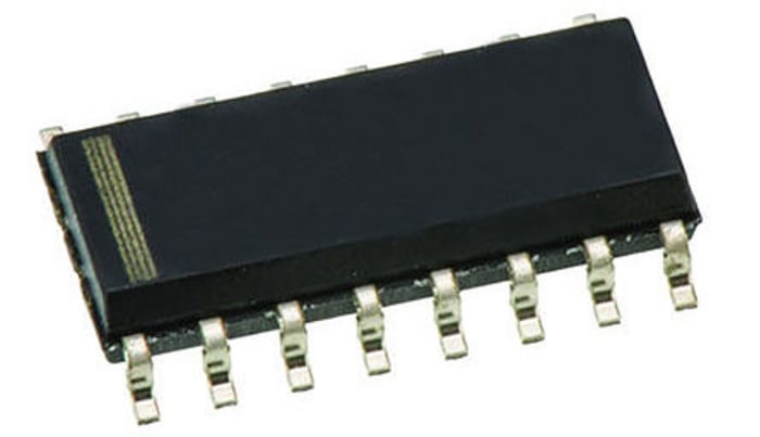
A range of 74HC Family CMOS Logic Counters and Shift Registers from NXP. The 74HC Family use silicon gate CMOS technology to achieve operating speeds similar to the LSTTL family but with the low power consumption of standard CMOS integrated circuits.

Ideate. Create. Collaborate
JOIN FOR FREE
No hidden fees!


Informações de estoque temporariamente indisponíveis.
P.O.A.
Each (In a Tube of 50) (Sem VAT)
50
P.O.A.
Each (In a Tube of 50) (Sem VAT)
Informações de estoque temporariamente indisponíveis.
50
Ideate. Create. Collaborate
JOIN FOR FREE
No hidden fees!
Documentos Técnicos
Especificações
Brand
NexperiaProduct Type
Shift Register
Mount Type
Surface
Maximum Supply Voltage
6V
Minimum Operating Temperature
-40°C
Maximum Operating Temperature
125°C
Standards/Approvals
RoHS
Detalhes do produto
A range of 74HC Family CMOS Logic Counters and Shift Registers from NXP. The 74HC Family use silicon gate CMOS technology to achieve operating speeds similar to the LSTTL family but with the low power consumption of standard CMOS integrated circuits.
Ideate. Create. Collaborate
JOIN FOR FREE
No hidden fees!